
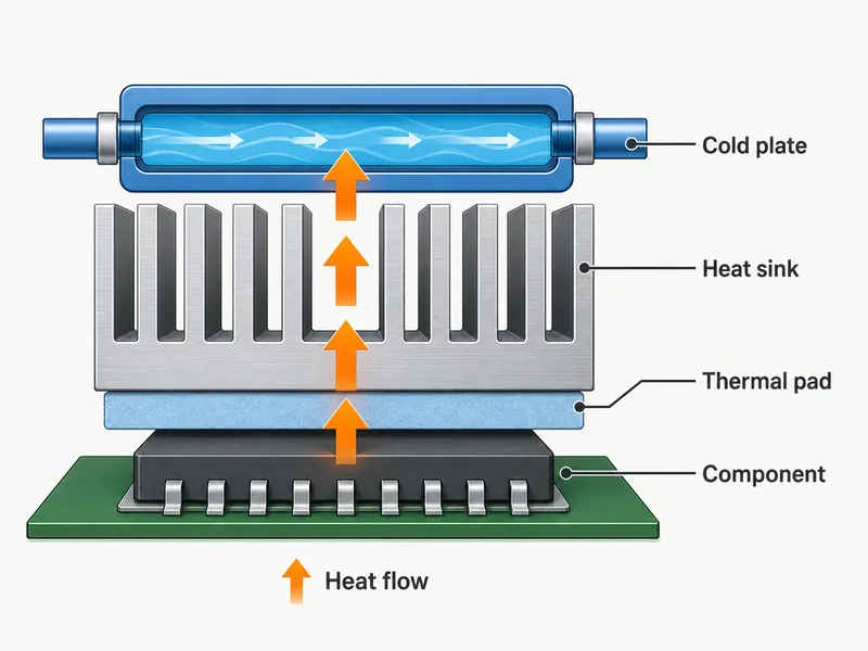
A thermal pad improves PCB performance by replacing the insulating air gap between a hot component and its heat sink with a conformable, solid path that conducts heat. At Trumonytechs we build thermal pads and liquid cooling plates as part of a wider thermal interface materials stack for battery-pack and power-electronics assemblies. So for a thermal engineer the working question is rarely whether to manage heat. It is which interface material matches the gap, the clamping stress, and the insulation the board actually needs.
The sections below explain how thermal pads work on a PCB, how to choose one by thermal conductivity, thickness, and electrical insulation, when a pad beats thermal paste, and how to install it without losing that performance. They do not cover cold-plate channel design, PCB copper and thermal-via layout, cell-format or pressure-drop trade-offs, or the datasheet values of any specific Trumonytechs model. Those depend on the board and the pack it sits in, and are set case by case.
Introduction to Thermal Interface Materials
A thermal interface material carries heat across a joint that would otherwise trap air. A thermal pad is the solid, pre-formed member of that family. Two mating surfaces that look flat still touch at only a few high points, so the rest of the joint fills with air. Air conducts poorly, around 0.026 W/m·K, while the metals it separates conduct hundreds of times better. That thin trapped layer ends up dominating the thermal resistance of the whole stack.
Whether a pad also isolates the two sides electrically depends on the product, not on the category. Many pads use a silicone or non-silicone binder loaded with fillers such as ceramic or metal oxide to raise heat transfer while staying dielectric. Others use conductive fillers like graphite and are not insulators. Do not read insulation from the words “thermal pad” or from a filler name. Where a pad can touch exposed pins or traces, confirm whether it is electrically conductive and check its rated dielectric strength.
Why PCB Thermal Management Affects Reliability
Heat that is left unmanaged can push components past their rated temperatures and drive expansion mismatch between the materials on the board. Semiconductors, capacitors, and integrated circuits each carry a working temperature range. Running above it may change their electrical behaviour before it causes outright failure, so a device that only drifts out of spec can already disturb timing or memory.
Thermal cycling adds a slower path. When copper, laminate, solder, and component bodies heat and cool at different rates, the mismatch shows up as mechanical stress at joints. Over enough cycles, that stress can crack solder or lift pads. How many cycles the assembly survives depends on the device ratings, the temperature gradient, and the cycle range, which is the core reason thermal management matters on a dense PCB.
Where Thermal Pads Fit in the PCB Heat Path
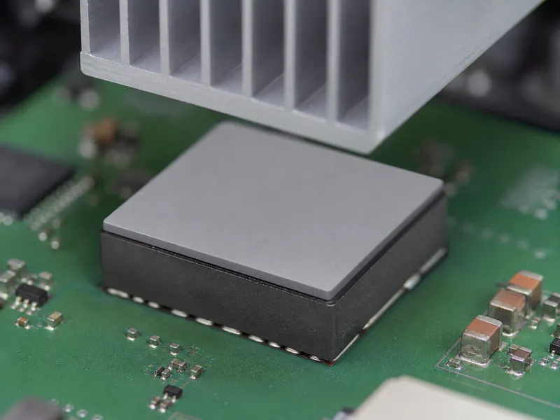
A thermal pad belongs at one specific place: the contact between a heat-generating component and its heat sink or cold plate. Its job there is to fill the microscopic gap that surface roughness and flatness tolerance leave behind. On a real assembly the two faces are never perfectly flat, so the pad has to conform under clamping pressure and stay in contact across the whole footprint. It earns its place wherever there is a measurable, repeatable gap that a rigid heat sink cannot close on its own.
For higher heat loads the pad is one stage in a longer path. In an EV or energy-storage battery pack, heat often moves from a board-level device or power module through the pad into a heat sink or structural member, and then into a liquid loop. Trumonytechs supplies liquid cooling plates for that downstream stage. Size the sink or cold plate behind the pad to carry the load, and treat the pad as the interface that gets heat off the component consistently.
Selecting a Thermal Pad: Conductivity, Thickness, and Insulation
Start a pad selection from the joint, not the datasheet: fix the gap and the required insulation first, then choose conductivity and thickness to suit them. These three variables interact, and reading one number off a datasheet is the most common way to under-serve a design. The sub-sections below take them in the order that usually matters.
Thermal conductivity
Higher bulk conductivity lowers the pad’s share of thermal resistance, but a datasheet figure is a test-method value, not a free-space property. Commercial pads commonly run from roughly 1.5 up to about 15 W/m·K, depending on the filler system, with the higher numbers coming from more heavily loaded composites. Those values are usually measured under a steady-state standard such as ASTM D5470, ASTM International’s test method for the thermal transmission properties of thermally conductive electrical insulation materials. Two pads are only comparable when they were characterised the same way. Read a stated W/m·K as a benchmark, then confirm real thermal resistance at your own pressure and bond line.
Thickness and compression
Match pad thickness to the gap, and plan to compress it. Pads come in a range of thicknesses, commonly from about 0.5 mm up to several millimetres. A pad is usually chosen slightly thicker than the nominal gap so clamping compresses it, often in the region of 20 to 50 percent per the manufacturer’s datasheet. That compression squeezes out air and seats the pad against both faces. Pushing past the rated compression to chase a thinner bond line has limits: the thermal gain may not continue, and the extra load transfers into the component and the solder joints under it.
Electrical insulation and compatibility
Treat insulation as a gate when the pad sits against exposed conductors. Where a pad can touch pins or traces, it has to hold off the working voltage without breaking down. In that position, select an insulating-type product with a stated dielectric strength or volume resistivity and its test conditions. Do not assume isolation from the category or the filler name. Silicone-based pads are common because they combine compliance with good dielectric behaviour, but verify compatibility against temperature, outgassing or oil bleed, the materials the pad contacts, and the design life; do not assume it will hold for the full service life.
Thermal Pad vs Thermal Paste
If the gap is real and repeatable, reach for a thermal pad; if the interface is nearly flat and you need the thinnest bond line, thermal paste can be the better fit. Both are thermal interface options, and the choice follows joint geometry and the production process more than any single conductivity figure.
| Factor | Thermal pad | Thermal paste |
|---|---|---|
| Gap it suits | Measurable, uneven, or tolerance-driven gaps | Small, flat, well-controlled gaps |
| Bond line | Thicker; set by pad thickness and compression | Thinner; can reach lower resistance |
| Assembly handling | Cut to shape, place, clamp; clean, pre-formed placement | Dispensed and spread; needs pressure and care |
| Reuse at rework | Depends on condition; a pad with compression set or damage is normally replaced per supplier guidance | Typically reapplied |
| Thermal-cycling risk | Can take a compression set or creep; verify by formulation and conditions | Can pump out over cycles; verify by formulation and conditions |
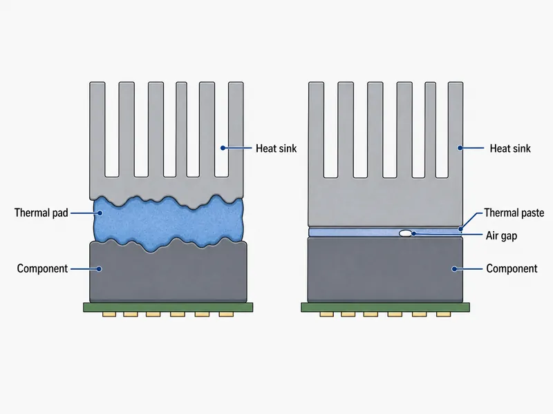
For an uneven or tolerance-driven gap, a pad is usually the more repeatable production choice because it fills the gap consistently. Where the interface is flat and the priority is the lowest resistance, paste can win, provided the process controls pressure and the design accounts for pump-out over thermal cycles. Confirm reuse and cycling behaviour against the specific material and its operating conditions; neither is guaranteed by category.
Installation Steps and Common Mistakes
Installation decides whether a well-chosen pad performs, and it starts with clean, flat contact faces. Most losses trace back to a few avoidable mistakes, so the sequence below keeps the thermal path intact from component to sink.
- Clean both faces so no dust, oil, or residue sits between the pad and the metal, since contamination adds resistance where you are trying to remove it.
- Measure the contact area and cut the pad to cover the full footprint without stretching it, because stretching thins the material and changes how it behaves.
- Remove any protective film and lay the pad flat over the component with no folds or overlaps, which would trap air and create hot spots.
- Apply uniform pressure to seat the pad and drive out trapped air, keeping compression within the pad’s rated range.
- Fit the heat sink or cooling module squarely and secure it with the intended clamps or screws so contact pressure stays consistent.
- Inspect for gaps or misalignment and, where it matters, monitor temperatures under load to confirm the interface performs.
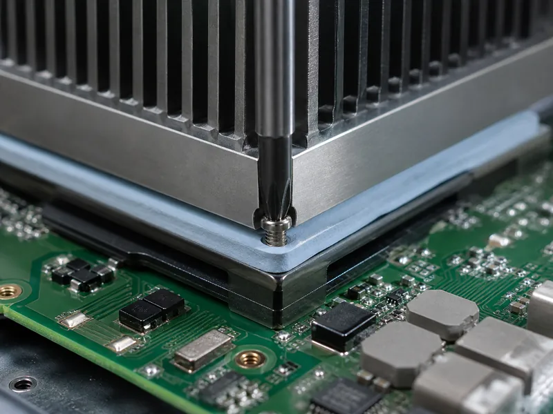
The recurring mistakes are stretching the pad, leaving air under it, and over-tightening. Stretching and air gaps raise resistance directly, and over-tightening trades a small thermal gain for mechanical load on the component. If a pad has to be removed, check its condition: one that has taken a compression set or shows damage is normally replaced, not reused, following the supplier’s guidance.
Conclusion
A thermal pad enhances PCB performance only when it is matched to the joint in front of you. Fix the gap and the required dielectric strength first, choose a thickness that compresses into that gap within its rated range, and treat a stated W/m·K as a comparison figure tied to a test method such as ASTM D5470. That last point is the easy one to get wrong: a higher datasheet number does not guarantee lower resistance in your assembly, so verify thermal resistance at your actual pressure and bond line.
If you are matching pads, gap fillers, or cold plates to a specific board or battery pack, contact Trumonytechs to work through the gap, pressure, and insulation constraints against the interface materials that fit them.
FAQ
Is a thermal pad or thermal paste better for a power module in a tight enclosure?
Match the choice to the gap. A pad suits a measurable or uneven gap and holds placement through thermal cycles, while paste suits a nearly flat interface where the thinnest bond line matters. In a tight enclosure with a real gap and clamping tolerance, a pad is usually the more repeatable production choice.
How thick should a thermal pad be?
Choose a pad slightly thicker than the gap so clamping compresses it into contact, often within the 20 to 50 percent range the datasheet specifies. A pad that is too thin leaves air, and one that is too thick adds mechanical load when compressed.
Can I trust the W/m·K value on a thermal pad datasheet?
Treat it as a benchmark measured under a test method such as ASTM D5470, not a guaranteed in-application value. Two pads are only comparable when characterised the same way, so confirm actual thermal resistance at your working pressure and bond line.
Does higher thermal conductivity always mean better cooling?
No. Real thermal resistance also depends on bond line thickness, contact pressure, and how well the pad fills the gap. A higher-conductivity pad that does not seat properly can underperform a lower-rated pad that makes full contact.
When should a thermal pad be inspected or replaced?
Trigger inspection or replacement by condition, not a fixed calendar. Check when a component trends hotter, after any disassembly event, or when the pad shows compression set, drying, cracking, or lost contact, and follow the supplier’s service-life and rework guidance. For sealed or non-serviceable assemblies, set the interface strategy during design validation instead of planning on field checks.
Further Reading
- ASTM D5470-17, Standard Test Method for Thermal Transmission Properties of Thermally Conductive Electrical Insulation Materials — ASTM International standard. Defines the steady-state method behind the W/m·K and thermal-resistance figures quoted for thermal pads, so it grounds the point that datasheet conductivity is a test-method value.
- Recent Advances in Thermal Interface Materials for Thermal Management of High-Power Electronics — peer-reviewed review, Nanomaterials (2022). Surveys TIM types and their conductivity ranges, supporting the distinction between everyday commercial pads and research-grade materials.
Related Articles
- Best Materials for Dissipating Heat in Electronics — Compares the material properties that make some interface and heat-spreading materials better at moving heat out of dense electronics.
- What is Phase Change Material? — Explains how phase change materials absorb and release heat to hold a stable temperature, an alternative interface class to solid pads.
- What is Thermal Grease? — Covers how thermal grease fills micro-gaps between a processor and heat sink, the paste option weighed against pads in this guide.