

A carbon nanotube thermal interface material uses aligned or dispersed carbon nanotubes to carry heat across the gap between a heat source and a heat sink. Its appeal comes almost entirely from how well a single nanotube moves heat along its length. That property is striking on its own: simulations and measurements on individual tubes report axial conductivities well into the thousands of W/m·K. The catch matters more than the headline number, though. Those values belong to one isolated tube. A finished layer built from many tubes performs far lower, because heat has to cross the contacts between the tube tips and the mating surfaces. For a battery-pack or power-electronics engineer, that gap between intrinsic conductivity and delivered performance is the whole story. It explains why these materials remain a research and specialty option today, not yet a shelf part.
What a Carbon Nanotube Thermal Interface Material Is
A carbon nanotube thermal interface material (CNT TIM) is a thin interface layer, built from carbon nanotubes, that sits between a component and its cooling surface to move heat and fill microscopic air gaps. The nanotubes usually stand as a dense forest grown perpendicular to the surface, so heat travels along the tube axis from the hot side toward the cold side. In other formats the tubes are pressed into sheets or blended into a polymer or metal matrix instead of grown as a standing array.
The reason the format matters is that a TIM’s job is contact, not bulk conduction. Any interface between two solid surfaces traps air in the surface roughness, and air is a poor conductor. The interface material has to be both conductive and compliant enough to conform under modest assembly pressure. Carbon nanotubes are attractive here because they are compliant along their length and can deform to absorb differences in thermal expansion between the parts they bridge, a known weakness of rigid solder-type interfaces.
Because the tubes can be grown directly on a metal substrate, a CNT array also sidesteps two failure modes that greases and some phase-change materials suffer over time. Pump-out and voiding, where the interface material is gradually squeezed out or leaves dry gaps under thermal cycling, are much less of a concern when the conductive path is anchored to the surface and no longer flows between the parts.
Why Single-Tube Conductivity Overstates Real CNT TIM Performance
Treat the intrinsic conductivity and the delivered conductivity as two separate quantities, because conflating them is the most misread fact about this material. Molecular-dynamics work on an isolated single-walled tube has put axial thermal conductivity as high as roughly 6600 W/m·K at room temperature. Measurements on individual multi-walled tubes have exceeded 3000 W/m·K. Both figures describe one pristine tube along its length, not a layer you can clamp between a cell and a cold plate.
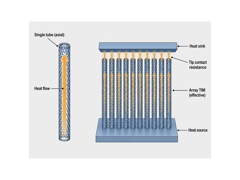
The effective conductivity of an assembled CNT array TIM lands one to two orders of magnitude below the single-tube value. Reported CNT-array results are on the order of tens to a couple hundred W/m·K, and those are research figures, not a general product specification. Two effects drive the drop. A grown array is mostly empty space, so the fraction of conductive material through the layer is low. More important, heat has to pass from the tube tips into the opposing surface, and that contact is where most of the resistance sits.
Interface resistance, not the conductivity of the tubes, is the number an engineer should track. The best laboratory arrays have reported interface resistance on the order of 1 mm²K/W, which is genuinely competitive. Those results depend on how the tips are bonded to the mating surface, not on the raw conductivity of the nanotubes. When you read a specification, ask for the through-plane thermal resistance of the assembled joint at a stated pressure. A conductivity figure quoted without that context describes the tube, not the product.
Types of Carbon Nanotube Thermal Interface Materials
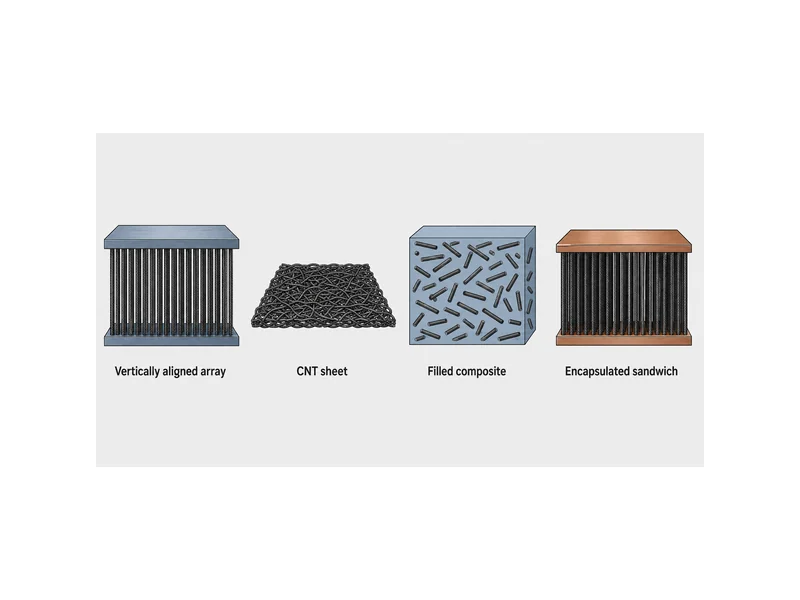
Carbon nanotube thermal interface materials come in a few structural families, and each trades manufacturability against how well it solves the contact problem. Knowing which format a supplier is offering tells you more about real performance than any single conductivity claim.
Vertically aligned CNT arrays
Vertically aligned CNT arrays (VACNTs) are dense forests of tubes grown perpendicular to a substrate, so the high axial conductivity points straight through the joint. Aligning the conductive direction with the heat-flow direction is the structural advantage of this format, but it does not settle real performance on its own: the joint resistance still depends on how well the tube tips contact the opposing surface, how thick the array is, and the pressure and bonding at the interface. Their weakness is that in-plane conductivity is poor, so they spread heat sideways badly, which limits their usefulness for smearing out concentrated hot spots.
CNT sheets and papers
CNT sheets and buckypapers are freestanding films of entangled or partially aligned tubes that can be handled and placed like a conventional pad. They are easier to integrate than a grown array because they do not require growing tubes on the actual part, but the random or in-plane orientation gives up much of the through-plane advantage that makes nanotubes interesting for a TIM.
CNT-filled composites and hybrid films
CNT-filled composites disperse nanotubes into a polymer, grease, or metal matrix to raise the conductivity of an otherwise conventional interface material. Adding high-aspect-ratio tubes creates extra conduction paths through the matrix, so these products behave like an improved gap filler, with the nanotubes reinforcing a conventional matrix instead of forming a pure nanotube layer. Hybrid films go a step further by pairing nanotubes with graphite or another carbon material such as a carbon fiber thermal interface material to combine through-plane and in-plane transport. The bonding between the two carbon phases then becomes its own source of resistance.
Encapsulated and sandwiched CNT arrays
Encapsulated arrays wrap or solder a nanotube forest between metal foils to protect it and to fix the tip contacts, which is the format closest to standard electronics packaging. One peer-reviewed study in Nano Research reported a copper–VACNT–copper sandwich, joined by a two-step soldering method, that achieved a 17 °C temperature reduction compared with state-of-the-art commercial TIMs in its test. That approach directly attacks the contact-resistance problem by bonding the tips instead of relying on dry pressure contact.
What Limits Real-World CNT TIM Performance
Manufacturing and integration, not the physics of the tubes, set the real limits on CNT thermal interface materials. Four constraints decide whether a given product is usable, and each maps to a variable you can check before designing it in.
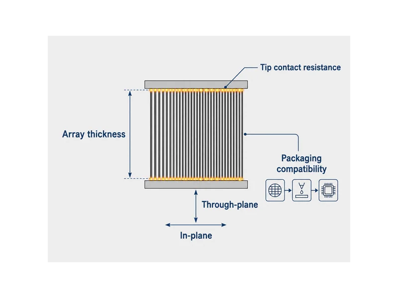
Contact resistance at the tube tips is the dominant limiter, and it is the variable to verify first. Because a dry array touches the opposing surface at scattered points, the through-plane resistance is set by that contact quality far more than by tube conductivity. Bonding the tips, by soldering, metallizing, or chemically functionalizing the interface, is what turns a promising array into a competitive joint, so any performance claim should specify how the tips are attached.
Growing long, dense tubes on a real metal substrate is difficult, which limits achievable thickness. The catalyst needed for growth tends to diffuse into a metal surface at growth temperature and shut the process down early, so arrays are often shorter than a designer would like for filling a large or uneven gap. When the gap between parts is large or the flatness is poor, a short array may not conform enough to make full contact.
Process compatibility with standard packaging is a third constraint. The high-temperature environment used to grow vertically aligned arrays is harsh and does not sit easily inside a normal device assembly flow, which is one reason encapsulated and pre-bonded formats have drawn attention. If a material has to be grown directly on your part, that requirement alone can rule it out.
Directional conductivity is the fourth item to weigh against your heat map. A vertically aligned array is excellent through the joint but weak in-plane, so it moves heat straight across the interface but does little to spread a localized hot spot. For a design that needs lateral heat spreading, a different interface strategy or a hybrid structure may serve better.
Where Carbon Nanotube Thermal Interface Materials Fit in Battery Thermal Design
A small commercial base exists for these materials, but it is still specialized, so treat them as an emerging option and not a drop-in replacement for established interface materials. A handful of suppliers offer them. Carbice, based in Atlanta, sells aligned-carbon-nanotube thermal pads aimed at electronics and aerospace. SHINKO has published a CNT TIM in development, with sheet sizes up to 50 by 50 mm and thicknesses of roughly 0.1 to 0.15 mm. What decides whether the technology is a candidate for a given build is availability at those sizes and formats, not a laboratory conductivity record.
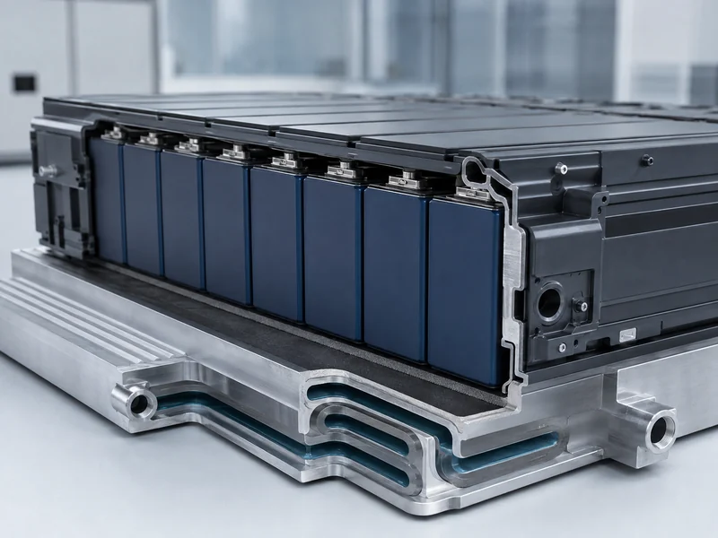
For an EV or energy-storage pack, three questions decide whether a CNT TIM can go in: the gap and flatness at the cell or module, the assembly stress and thermal cycling the interface must survive, and whether it fits an automated dispensing or placement step at production volume. These are the same variables that govern any interface choice in the cell-to-coolant path. Grown-array CNT materials are hard to reconcile with those pack-level realities today. Established gap pads, gels, and greases fit the existing assembly flow more easily, which keeps them the workable choice for the high-performance thermal interfaces that move heat from cells into a cold plate.
A supplier like Trumonytechs works in that practical framing, matching a TIM to the gap, curing behavior, insulation status, and bonding need of a specific pack. A single headline number rarely captures those variables. Carbon nanotube materials are still worth watching for the cases where their through-plane strength and compliance solve a problem the incumbents cannot, particularly in dense power electronics. Even then the selection logic does not change: verify the assembled joint resistance, the format, and the integration step before the tube-level number.
Conclusion
The useful takeaway is that a CNT TIM earns its value in the assembled joint, not in the conductivity of a lone tube, and reading it the other way is the most common mistake. Intrinsic conductivity in the thousands of W/m·K is real. The delivered interface resistance, though, depends on how the tube tips are bonded to the mating surface, how thick and conformable the array can be made, and whether the format survives a normal assembly flow. Judge any candidate by its through-plane resistance at a stated pressure and by how it is integrated, and the technology sorts itself into the narrow set of applications where it currently earns its place. For a battery pack, that means confirming gap, flatness, assembly stress, and production method against a real interface layer before the nanotube conductivity ever enters the conversation.
FAQ
How thermally conductive are carbon nanotubes?
An individual carbon nanotube is extraordinarily conductive along its length, but a finished interface material is not. Simulations put a single-walled tube as high as about 6600 W/m·K at room temperature, and single multi-walled tubes have been measured above 3000 W/m·K. Once tubes are assembled into an array TIM, the effective conductivity drops by one to two orders of magnitude below those single-tube values, so the finished layer behaves nothing like a lone tube.
Why don’t carbon nanotube thermal interface materials reach their theoretical conductivity?
Contact resistance at the tube tips is the main reason a CNT TIM falls short of the single-tube figure. Heat has to cross from the ends of the nanotubes into the opposing surface, and a dry array touches at scattered points. Those scattered contacts, more than the tubes themselves, govern the joint resistance. Bonding the tips by soldering, metallizing, or functionalizing the interface is what closes much of the gap.
Is a vertically aligned CNT array better than a graphite pad?
The direction of the heat you need to move decides this one. A vertically aligned CNT array puts its conductive axis straight through the joint, which suits through-plane transport, though the delivered result still hinges on tip contact, thickness, and pressure. Its in-plane conductivity is poor, so it spreads lateral hot spots badly. A graphite sheet is the opposite, strong in-plane and weaker through-plane, so your heat map should decide the better format.
Can carbon nanotube thermal interface materials be integrated into standard electronics packaging?
Integration hinges on two things: whether the material comes in a pre-encapsulated or pre-bonded form, and whether its growth step is separated from device assembly. A grown array needs a high-temperature process that does not sit easily inside a normal packaging flow, which is why encapsulated formats, nanotube forests fixed between metal foils, are the ones closest to standard packaging. Where the tubes must be grown directly on the part, that requirement alone can keep the material out of a conventional assembly line.
Can carbon nanotube thermal interface materials be used in EV battery packs?
Carbon nanotube TIMs are not yet a routine choice for EV battery packs, and the limit is more about integration than performance. A pack interface has to match the gap and flatness at the cell or module, survive assembly stress and thermal cycling, and fit an automated production step. Grown-array formats are hard to reconcile with those constraints today, so established gap pads, gels, and greases remain the practical fit for cell-to-coolant paths while nanotube materials are proven out for niche high-flux cases.
Further Reading
- Encapsulated carbon nanotube array as a thermal interface material compatible with standard electronics packaging (Nano Research, 2023) — peer-reviewed study. Supports the point that bonding and encapsulating the array attacks contact resistance and can beat commercial TIMs in through-plane performance in its test.
- Carbon nanotube-based thermal interface material patent, publication US20200404809A1 (later granted as US11291139B2), via Google Patents — a primary patent disclosure from a CNT-TIM developer. Documents array and multilayer construction methods and the emphasis on tip contact and interface resistance; read as the applicant’s own filing, not an independent test.
Related Articles
- Thermal Interface Materials Types & Characteristics — Maps the main thermal interface material families and their characteristics, useful for placing CNT TIMs among established options.
- Thermal Gel vs Thermal Paste — Breaks down how thermal gel and thermal paste differ in composition and conductivity when matching an interface material to a build.
- Thermal Gel vs. Thermal Pad: Key Differences Explained — Explains how gels and pads fill surface gaps differently, helpful when a grown CNT array is not yet practical for an assembly.
- What Thermal Paste Is for Computers — Covers what thermal paste does at CPU and GPU interfaces and the variables that keep temperatures in check.
- When to Use Thermal Gel? — Describes when a thermal gel is the right interface choice for a given cooling need.