
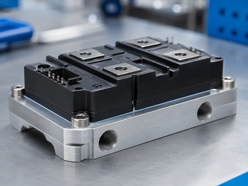
Thermal interface materials for power electronics applications carry heat across the imperfect contact between a power semiconductor and its heat sink or cold plate. Choosing one is a system decision, not a search for the highest number on a datasheet. Two ground surfaces that look flat still touch across only a small fraction of their area. The air trapped in the remaining gaps conducts poorly, at roughly 0.025 W/m·K, so something better has to displace it. A peer-reviewed review of high-power electronics reports steady-state heat fluxes on the order of 150–200 W/cm², and pulsed transients above 400 W/cm². At those fluxes a thin, poorly matched interface can dominate the temperature rise, even when every other layer is well engineered. The sections below cover what the interface does, why conductivity alone misleads, which material families are available, and how gap, insulation, cure, and assembly method decide the answer.
What a Thermal Interface Material Does in a Power Electronics Stack
A thermal interface material occupies the one layer in a power module stack that assembly, not physics, leaves you free to control. Heat leaves the die and passes through the chip attach, the substrate (often a direct-bonded-copper layer), and the baseplate, then crosses into the heat sink or liquid cold plate. Each of those layers has a fixed material and geometry once the module is built. The joint between baseplate and cooler is different: it is filled at assembly, and its resistance depends on how well that fill is done. Because it is both variable and often poorly controlled, this joint is a frequent contributor to the total thermal path. How large a contributor it is depends on the specific stack, so check it by measurement instead of assuming it.
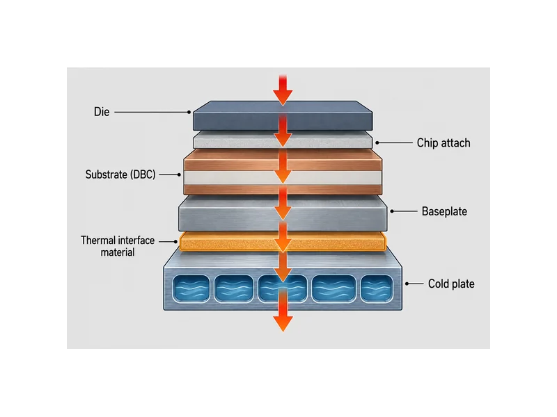
The interface matters because contact resistance scales with how much real metal-to-metal area you achieve, and machined surfaces give you little of it. Surface roughness, warpage from soldering, and clamping pattern all leave microscopic and macroscopic voids. A TIM fills those voids so heat conducts through solid material instead of stalling in air. The same power module can then run measurably cooler or hotter depending on what fills that gap and how it went in. Confirm the size of that effect for your own stack by measuring case or junction temperature under load.
Why Higher Conductivity Alone Won’t Lower Junction Temperature
Chasing the highest bulk thermal conductivity is a common way to over-spend and still miss a temperature target. The number that reaches the junction is thermal resistance across the whole joint. That resistance depends on bond line thickness and contact resistance at least as much as on the material’s conductivity. A high-conductivity paste laid down too thick can lose to a modest material used well, and so can a stiff pad that will not conform under the available clamping force.
Bond line thickness is a lever that is easy to overlook. Greases can be driven down to tens of microns under pressure. A gap pad often has to stay several times thicker to bridge an uneven interface, and resistance rises roughly with that thickness. For high-power modules a common target is a low joint resistance, often cited as under about 1.0 K·cm²/W. Treat that as a condition-dependent figure, not a standard. You reach it by matching the material’s compliance and application to the real gap, not by reading the largest W/m·K on the shelf. Verify the result as installed resistance or measured case temperature under load, because bulk conductivity quoted in isolation does not predict what the assembly delivers.
TIM Families Used in Power Electronics and Their Trade-offs
Each TIM family trades thermal performance against gap tolerance, electrical behavior, and reworkability. That is why the right family follows from the interface before it follows from a conductivity spec. Their types and characteristics overlap enough that gap and assembly usually decide the choice, not headline conductivity. The table gives typical, condition-dependent ranges for comparing families on the dimensions that drive the decision.
| TIM family | Bulk conductivity (W/m·K) | Heat-flow direction | Typical bond line / gap | Electrically insulating? | Reworkable? | Best fit in power electronics |
|---|---|---|---|---|---|---|
| Thermal grease / paste | ~2–10 (enhanced grades higher) | Through-plane | Tens of microns under pressure | Grade-dependent | Limited; messy, pump-out risk | Flat, well-clamped module-to-cold-plate joints |
| Gap pad | ~1–5 | Through-plane | Fractions of a mm to a few mm | Insulating grades available | Yes | Uneven gaps, lower assembly pressure |
| Phase-change material | Grade-dependent | Through-plane | Thin, self-leveling above transition | Grade-dependent | Semi-permanent | High-power flat joints needing low, repeatable resistance |
| Gap filler (dispensed) | ~1–4 | Through-plane | Conforms to the gap | Grade-dependent | Limited once cured | Large or uneven tolerances |
| Thermally conductive adhesive | ~1–4 (specialty grades higher) | Through-plane | Thin to moderate | Grade-dependent | No — structural bond | When structural bonding is required |
| Graphite / carbon film | High in-plane; lower through-plane | In-plane spreading | Very thin | Often electrically conductive | Moderate | Thin, flat joints where lateral spreading helps |
Installed joint resistance is the metric that decides junction temperature. Published values are not reported on a common basis across these families, so treat the conductivity column as an order-of-magnitude guide and confirm resistance as installed. Greases and phase-change materials suit a flat, firmly clamped interface, where they reach a thin bond line and hold a low resistance under load. Pads and dispensed gap fillers earn their place where the gap is larger or uneven and the clamping force is limited. They trade some conductivity for the compliance to fill the space without stressing the module. Adhesive-style materials add structural bonding or vibration tolerance where the joint has to carry load, at the cost of reworkability.
Matching a TIM to the Interface: Gap, Flatness, Assembly Stress, and Automation
Start selection from the interface’s gap and flatness. Those set the compliance the material needs before conductivity is worth comparing. A joint held within a few tens of microns and clamped hard suits a thin grease or phase-change film. A warped baseplate or a loose-tolerance stack needs a gap pad or a dispensed gap filler that conforms without high pressure. Measure the real gap and its variation across the footprint, not the nominal design value, because that measurement often changes the answer.
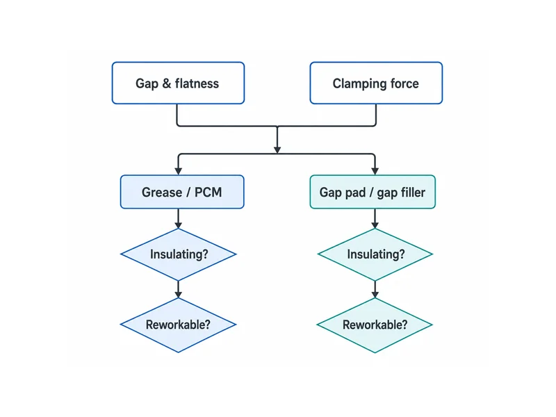
Assembly stress can quietly rule out otherwise-good materials. A stiff, high-conductivity pad can transmit force through a large SiC or IGBT module. Whether that force is enough to bow the substrate or fatigue solder joints over thermal cycles depends on the module construction and clamp design. Ask the supplier for compression-deflection data and weigh it against the force your mechanical design can actually apply. The compliant option is sometimes the more reliable one, even at lower conductivity.
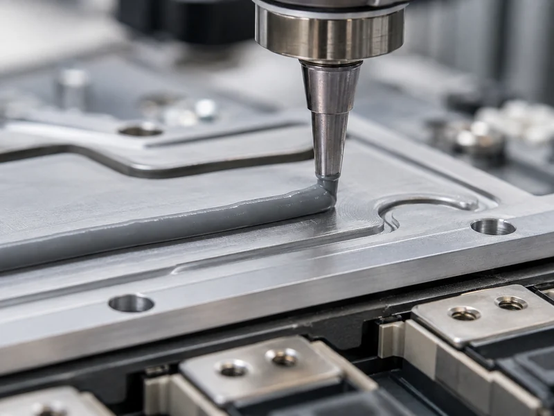
Automation method decides which materials stay repeatable at volume. Dispensed gap fillers and stencil-printed greases suit automated lines and give unit-to-unit control of bond line. Hand-placed pads trade some of that control for simpler tooling. A material a technician applies well by hand can vary more once it is placed at production volume, so qualify the application method with unit-to-unit bond-line or resistance data before committing. When interface, gap, insulation, and process are all on the table, ranking those constraints is what makes the selection defensible, not sorting by conductivity.
Electrical Insulation, Cure, and Reliability Under Thermal Cycling
Decide the electrical role of the interface first, because it can eliminate whole families of material. Where the TIM sits between a live baseplate and a grounded cooler and provides isolation, it must be electrically insulating with margin. Insulating grades are commonly rated to dielectric strengths of several kV/mm. The usable figure depends on the specific product and thickness, so confirm it on the datasheet. Where isolation is handled elsewhere in the stack, electrically conductive options such as metal-loaded or graphite materials open up. The design problem then becomes keeping them clear of nearby traces.
Cure and bonding behavior set whether the joint is serviceable. Non-curing greases, gels, and pads let you rework or replace a module. A thermally conductive adhesive cures into a structural bond that resists vibration, but it is generally not reworkable without damaging the joint, depending on the adhesive. Choose a curing material only when the bond is a requirement, because it changes repair, warranty handling, and line rework.
Reliability over thermal cycles is where a good day-one measurement can still fail in service. Greases can suffer pump-out and dry-out as repeated expansion and contraction work material out of the joint. Pads can take a compression set, and mismatched coefficients of thermal expansion can drive delamination or voids that raise resistance over time. How quickly any of these appear depends on the material chemistry, clamp pressure, bond line, and the temperature range and cycle profile the part sees, so treat them as risks to qualify, not certainties. ASTM D5470 gives a common basis for measuring steady-state heat transfer and thermal resistance under specified conditions. It does not reproduce aging, so pair it with pump-out and thermal-cycling data for the temperatures your power electronics actually see.
Applying TIMs Across the Cell-to-Coolant Path in EV and ESS Packs
In an EV or ESS pack a TIM appears in more than one heat path, and those paths are not a single series chain. Cells reject heat through their own interface into a cold plate or cooling structure: cell to TIM to cold plate. The power electronics form a separate path, where the semiconductor junction moves heat through its package and baseplate, through a TIM, and into a heat sink or cold plate. The traction inverter and its IGBT or SiC modules are not a mandatory layer between the cells and the coolant. They are a parallel load on the same cooling architecture. Chosen well, both interfaces keep their own path’s resistance within budget under the pack’s duty cycle.
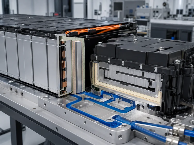
The interface form differs by location, so confirm it against the actual package and mounting instead of assuming it. Hard-clamped power-module baseplates can present the flat, well-controlled joints where a thin grease or phase-change film pays off. Battery-side electronics and control boards more often present uneven gaps that suit compressible gap fillers and pads, but verify flatness, clamping, and gap on the real assembly. Matching each interface to its cooler is where the pack-level payoff shows up, because the best-machined cold plate is wasted if the joint feeding it is thick or voided. Trumonytechs develops thermal interface materials and matched liquid cold plates for battery-pack and power-electronics cooling; explore our TIM solutions to pair a gap filler, pad, or dispensed material with the cooling component it sits against. The same discipline applies wherever the power electronics live, from a vehicle inverter to energy storage battery packs in data centers, where duty cycle and gap variation decide the material more than any single conductivity figure.
Conclusion
The interface, not the datasheet, should decide a thermal interface material for power electronics. Fix four constraints before you shortlist anything: the gap and its variation, the clamping force the mechanical design allows, whether the joint must insulate, and whether it must stay serviceable. Let those narrow the family, then let conductivity break the tie. Treating a high W/m·K rating as the goal is the trap, because bond line thickness, contact resistance, and cycling behavior are what the junction actually feels. Confirm the choice as installed resistance or case temperature under real load. Finally, qualify greases for pump-out over the pack’s service life against a defined cycle count, temperature range, clamping condition, and failure criterion, not a generic lifetime number.
FAQ
Do I need a thermal pad or thermal grease for an IGBT module?
Match the choice to the joint, not the module name. Thermal grease suits a flat, firmly clamped IGBT baseplate because it reaches a thin bond line. A thermal pad suits an uneven gap or a design with limited clamping force. Grease gives lower resistance when the interface cooperates; a pad trades some conductivity for compliance and easier, more repeatable placement.
What thermal conductivity do I actually need for a SiC power module?
The useful target is a low installed joint resistance, not a single conductivity number, because bond line thickness and contact resistance often matter more. For high-power modules, a joint resistance under roughly 1.0 K·cm²/W is a common goal. It is a condition-dependent target, reached by matching the material’s compliance and application to the real gap, not by buying the highest W/m·K on the shelf.
Can I use a phase-change material instead of grease for high-power modules?
Often yes. Phase-change materials are frequently chosen for high-power, flat joints because they soften above their transition temperature and reach a thin, low-resistance bond line. Where hand-applied grease varies from unit to unit, a phase-change film can hold a more consistent bond line, though you should confirm that for your own product and process. The trade-off is that the film is semi-permanent and needs a flat, well-clamped interface to perform.
How thick should the thermal interface bond line be?
Aim for the thinnest bond line the interface allows while still filling every void, since resistance rises with thickness. Greases and phase-change films can reach tens of microns under pressure on a flat joint, whereas an uneven gap forces a thicker pad or gap filler. Measure the actual gap across the footprint rather than trusting the nominal value.
Does a power-electronics TIM need to be electrically insulating?
Only when the interface itself provides isolation between a live baseplate and a grounded cooler; then it must be insulating with dielectric margin for the applied voltage and thickness. Where isolation is handled elsewhere in the stack, electrically conductive materials become options, but the design then has to keep them clear of adjacent conductors.
Further Reading
- Recent Advances in Thermal Interface Materials for Thermal Management of High-Power Electronics — peer-reviewed review (Micromachines, via NCBI PMC). Supports the high-power heat-flux figures and the conductivity ranges used to frame the material trade-offs above.
- Advanced TIMs Help Overcome Power-Density Thermal Challenges — industry technical media (Electronic Design). Background on how thermal interface materials address rising power density in modern power-electronics modules.